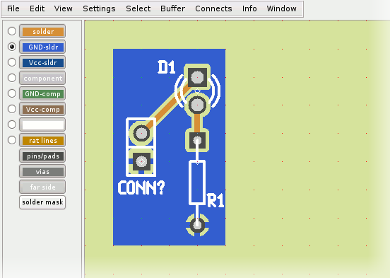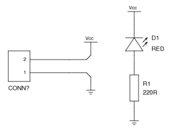
This is a short tutorial on using gEDA for round-trip engineering.

Start gschem with:
gschem my-schematic.sch
[I] to insert a part. The text input focus will be in the Filter field. Start typing a part code and the tree in the main view will simmer down to show only matching parts. Some common parts are:
resistor, capacitor, diodepnp, npngnd, vcc, vdd, 12V-plusconnector[OK] to select a part and then use the left mouse button to add parts of that kind. Press [Esc] when finishedD? next to the part is the reference designator, or refdes. It can be selected independent of the part and edited with [E] then [X]. The size and alignment of the text can be changed in that dialog too[N] to start laying a net in order to connect parts. Press [Esc] when finished laying a net[A] twice when a net is selected. Nets with the same name are connected. Using Vcc or GND for net names causes the net to be connected to those railsSave the schematic and use:
refdes_renum my-schematic.sch
..to automatically number all reference designators that end with "?".
Some useful keys ( Note: "v, e" means press [V] then [E])
| Keys | Effect |
|---|---|
| v, e | View Extents: Zoom so that the whole schematic is in view |
| w | Choose an area of the view to zoom in to |
| u | Undo |
| Shift+R | Redo |
Some useful keys that affect the selected parts:
| Keys | Effect |
|---|---|
| m | Move |
| Delete | Delete |
| e, r | Rotate |
| e, i | Mirror |
| e, c | Copy |
| e, e | Edit attributes |
| a, a | Add attribute |
| t, u | Auto-number text |
Common attributes:
| Attribute | Purpose |
|---|---|
| footprint | Indicates the physical plan of the part on the PCB. DIP28N for example |
| value | The value of a resistor or capacitor. Used to generate the BOM |
Common footprints:
| Footprint | Usage |
|---|---|
| AXIAL_LAY s | s is the pin separation, e.g. AXIAL_LAY 300 |
| RADIAL_CAN d | d is the diameter of the package, not the pin separation. RADIAL_CAN 200 |
| TO92 | |
| TO220 | |
| DIP20 | For a 20-pin dual in-line package |
| JUMPER4 | For a 4-pin header |
| LED d | d is the outside diameter of the LED in mils, e.g. LED 197 for a 5mm LED |
| HEADER10_2 | 10-way header with 2 rows, i.e. 5x2 header |

Ensure that each part has a unique refdes and then:
gsch2pcb my-schematic.sch
Scan the output for errors ( which are usually about missing footprints), correct and then re-run. If gsch2pcb outputs:
...
/usr/bin/m4:stdin:22: bad expression in eval:  /4
...
..then possibly a footprint is LED-197 when it should be LED 197.
Open the new PCB with:
pcb my-schematic.pcb
Auto enforce DRC clearance but tick Crosshair shows DRC clearanceNew lines, arcs clear polygonsmy-schematic.net[O] to show the "rats nest", which shows which pins should be connected to which othersRoute Style before drawing lines. For home-made circuit boards, Line width and Clearance of 20 mils or greater is prudent[O] after drawing each line to see the rats nest get tidierPCB Log window shows how many rat lines remain to be routed and if any nets are shortedDesign Rule Checker checks that the layout meets the specifications in Preferences, SizesSome useful keys:
| Key | Effect |
|---|---|
F1 |
Via tool |
F2 |
Line tool |
F4 |
Text tool |
F5 |
Rectangle tool ( for ground pours) |
F9 |
Rotate tool |
/ |
Changes where the line bends |
m |
Move the element under the cursor to the current layer |
M |
Move selected elements to the current layer |
o |
Show the rats nest |
e |
Hide the rats nest |
Tab |
Show the other side of the board |
u |
Undo |
R |
Redo |
B |
Move selected elements to the other side of the board |
Sometimes the schematic changes after some of the PCB has been laid out.
Once the schematic has been updated, ensure that the latest changes to the PCB have been saved and then re-run:
gsch2pcb my-schematic.sch
gsch2pcb will edit my-schematic.pcb in-place to remove parts that have been deleted or had their footprint changed but it will put new parts and parts with new footprints in my-schematic.new.pcb. Assuming my-schematic.pcb is already open:
Load layout to reload the my-schematic.pcb fileLoad layout data to paste buffer to load the my-schematic.new.pcb fileDisperse selected elementsLoad netlist file if it has changed[O] to update the rats nest and then lay out the newly added partsA ground pour makes routing easier because GND traces need not be laid out at all. Where a ground plane is present on a four-layer board, the signal will return through the ground plane directly underneath the trace above. A more roundabout return can cause RF problems in high-frequency boards. Pours are still good for conserving etchant though.
Netlist dialog from the Window menuGND net so that it has a * next to it[O]New lines, arcs clear polygons is tickedNew lines, arcs clear polygons and draw lines to connect those pins to the ground pour that should be tied to GNDgEDA has a symbol creation guide.
To configure gschem to use a local component library, ensure that ~/.gEDA/gafrc contains something like:
(component-library "/home/neil/electronics/symbols")
Create a symbol with:
gschem BC549.sym
The .sym rather than .sch causes gschem to realise you'd like a symbol rather than schematic.
Add Pin to draw pins. Add boxes and lines too. For each pin:pinnumber and pinseq to the same value (counting up starting at 1)pintype to one of:
in: inputout: outputio: input/outputoc: open collectoroe: open emitterpas: passivetp: totem poletri: tristate (high impedance)clk: clockpwr: power/groundNeil Stockbridge <neil@example.com>gsymcheck -vv BC549.sym
Symbol Translate from the Edit menu and use a value of 0Add attributes above or to the right of the symbol otherwise they will be obscured when the symbol is translated.
When pcb has no footprint for your part, just make one!
mkdir ~/electronics/footprints/mine
..then in pcb, go to:
File , Preferences... , Library , Element Directories
..and change it to include:
~/electronics/footprints
..then make a file in ~/electronics/footprints/mine/BSA325.fp like so:
# Element( flags description blank blank mark_x mark_y text_x text_y text_direction text_scale text_flags
# Pin( x y thickness clearance mask drillhole name number flags
# ElementLine( x1 y1 x2 y2 thickness)
# ElementArc( centre_x centre_y radius_x radius_y startAngle deltaAngle thickness)  startAngle in degs, 0=East, +ve deltaAngle anti-clockwise
# Measurements are taken from the datasheet
#
Element( 0x00 "BS-A325* small seven-segment display" "" "BS-A325" 0 0 150 100 3 100 0x00)
(
  Pin(   0   0  60  70   0  28 "Common Anode"  "1" 0x101)
  Pin(   0 100  60  70   0  28 "f"             "2" 0x001)
  Pin(   0 200  60  70   0  28 "g"             "3" 0x001)
  Pin(   0 300  60  70   0  28 "e"             "4" 0x001)
  Pin(   0 400  60  70   0  28 "d"             "5" 0x001)
  Pin( 200 400  60  70   0  28 "Common Anode"  "6" 0x001)
  Pin( 200 300  60  70   0  28 "dp"            "7" 0x001)
  Pin( 200 200  60  70   0  28 "c"             "8" 0x001)
  Pin( 200 100  60  70   0  28 "b"             "9" 0x001)
  Pin( 200   0  60  70   0  28 "a"            "10" 0x001)
  ElementLine( -45 -70 -45 470 10)  # left, starting top-left going anti-clockwise
  ElementLine( -45 470 245 470 10)  # bottom
  ElementLine( 245 470 245 -70 10)  # right
  ElementLine( 245 -70 -45 -70 10)  # top
)
Values for thickness, drillhole and mask are diameters yet the clearance of a pin is specified as twice the minimum clearance, so a "clearance" of 30 tells the Design Rule Checker that there must be at least 15 mils between the edge of the pad and any other copper.
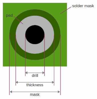
Thickness and clearance apply to DRC. Mask, thickness and drillhole apply to fabrication. Thickness is the diameter of the pad and "mask" the diameter of the hole in the solder mask:

When specifying drill diameters, add 19 mils to compensate for through-plating if having PCBs fabricated.
Don't forget when running gsch2pcb to specify the elements directory like so:
gsch2pcb -d ~/electronics/footprints twin-bcd.sch
The built-in Write image feature produces lacklustre results with bitmap formats. Here's how to get better results, even if in monochrome:

Write image... from the File menu. For Image type, choose Encapsulated Postscript and press [Save].eps file with GIMP. Choose Strong antialiasing for both Text and Graphics[R] to select the area of the schematic to be publishedCrop to Selection from the Image menuAutocrop Image from the Image menuScale Image from the Image menu[Scale] and then save the image"hole" flagFile > Export layout... [gerber]/tmp/ if desiredgerbv /tmp/<board-name>* to see all layers at once.sch and .pcb files are plain text files. They can be edited manually or processed with scripts to do things such as change the clearance of the pins of partsView, Displayed element name, Value and then go round selecting the values, pressing n and deleting the values. Don’t delete the designators or the descriptions otherwise round-trip engineering stops working